Typical applications of transparent conductive oxides (TCO’s) include touch panel contacts, energy conserving architectural windows, defogging aircraft and automobile windows, heat-reflecting coatings to increase light bulb efficiency, gas sensors, antistatic window coatings, EMC coatings, wear resistant layers on glass, cold mirrors, displays, electrochromics and photovoltaics.
The most widely used TCO is indium tin oxide although Al:ZnO has also emerged as a viable alternative.
The TCO deposition parameters play interdependent roles in the optimization of film properties. Principal among the deposition parameters are partial pressure of oxygen, substrate temperature, rate of deposition and material composition. Some processes require post deposition baking at 300-500° C in air to oxidize residual fractionated metal component and improve conductivity. For the closed field sputter process, a high energy plasma can be substituted for a high substrate temperature.
Closed field reactive magnetron sputtering produces dense, spectrally stable metal-oxide optical coating material with refractive indices typically close to that of the bulk material. Similarly closed field sputtered TCO`s produce low stress, transparent conductive thin films that are super-smooth with exceptional electrical and optical properties.
The quality of thin films of Transmitting Conducting Oxides (TCO’s) such as Indium Tin Oxide (ITO) is vital to the performance of a range of new products in high growth markets such as Electrochromics, OLED displays and also thin film photovoltaics based on either CdTe or CIGS absorbers. In many of the most exciting applications these devices are being applied to polymer substrates so it is vital that the processes provide excellent electrical, optical and mechanical properties while maintaining low temperature deposition. The CFM process produces ITO films that provide electrical conductivity of 10 ohm/sq with high optical transmission with a thickness of 360nm deposited at room temperature with no post annealing. Moreover, the deposited ITO thin films are super-smooth.
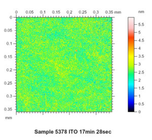
A CCI image revealing the metrology of a 365nm ITO film deposited at room temperature. The color scale shows the maximum height difference across the 0.35mm square sample area. The measured RMS roughness from this area is Sq=0.453nm (Data courtesy of Ametek Taylor Hobson).
Surface metrology studies using Coherence Correlation Interferometry (CCI) show that the RMS roughness of a 360nm film is typically less than 0.5nm even though the deposition rate exceeds 5 A/sec. Super-smooth ITO films are particularly desirable for OLED display devices.